ASIC puzzle
Recently, Jane Street put out a challenge to reverse engineer an ASIC design they had created, which I heard through a poster in the TinyTapeout Discord.

I decided to take a stab at it, in part because I had used the OpenRoad/LibreLane tools before and someone said that it would be easy to those that knew the tools.
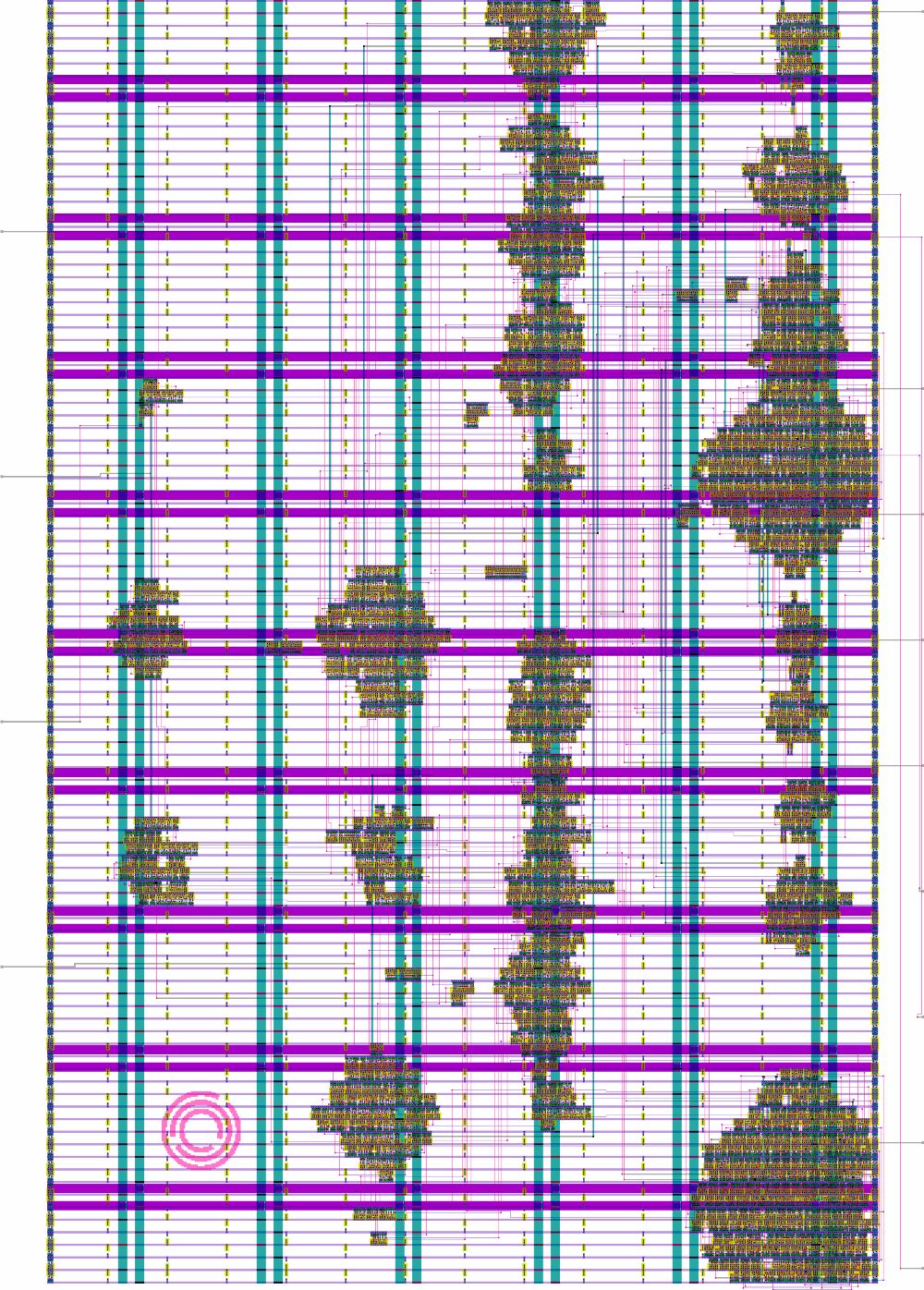
First things first, I needed to figure out what process the given IC design was in. Opening the GDS file in Klayout in viewer mode, I was surprised to find a cell hierarchy waiting for me!
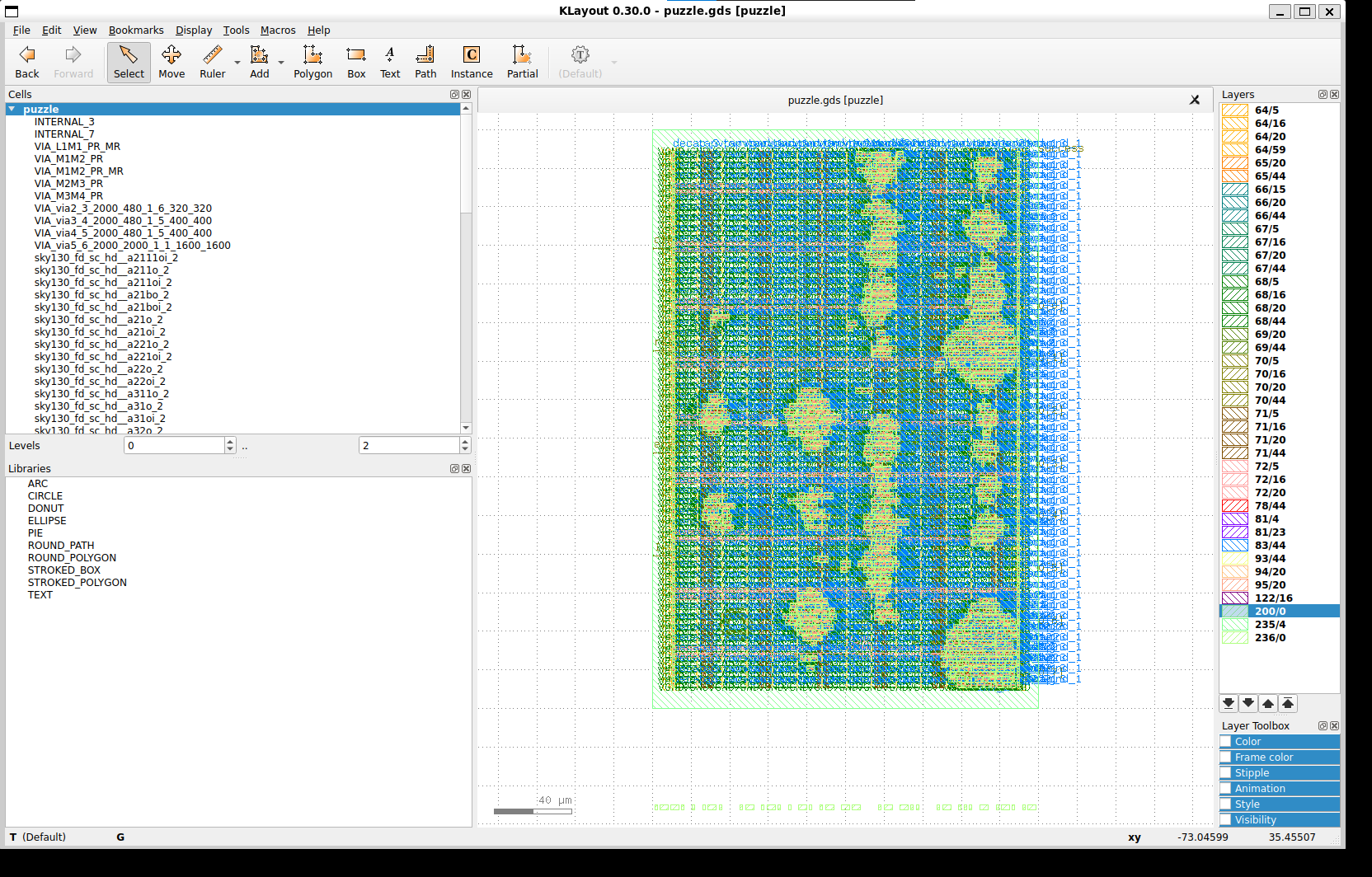
Plain as day, there’s the sky130 process standard cells listed on the cell hierarchy.
Most of the cells are for high density logic (sky130_fd_sc_hd*), and there’s also some VIA cells (which are used along with the metal to connect the inputs and outputs of each cell). However, this isn’t a fully clean capture.
I started off by attempting to load the file into my IC design software of choice: Magic VLSI. Though Klayout and the Cadence suite would likely be just as valid, Magic is quite efficient to use once you are used to it, and it is well supported if you are using an open source PDK (like sky130).
After setting up the PDK, I attempted a straight import of the GDS from the menu. However, there’s the following error

Perhaps it could be an intentional Easter egg?
The INTERNAL_3 and INTERNAL_7 are the marks in light green at the bottom of the actual design (so are not relevant to analyzing the design).
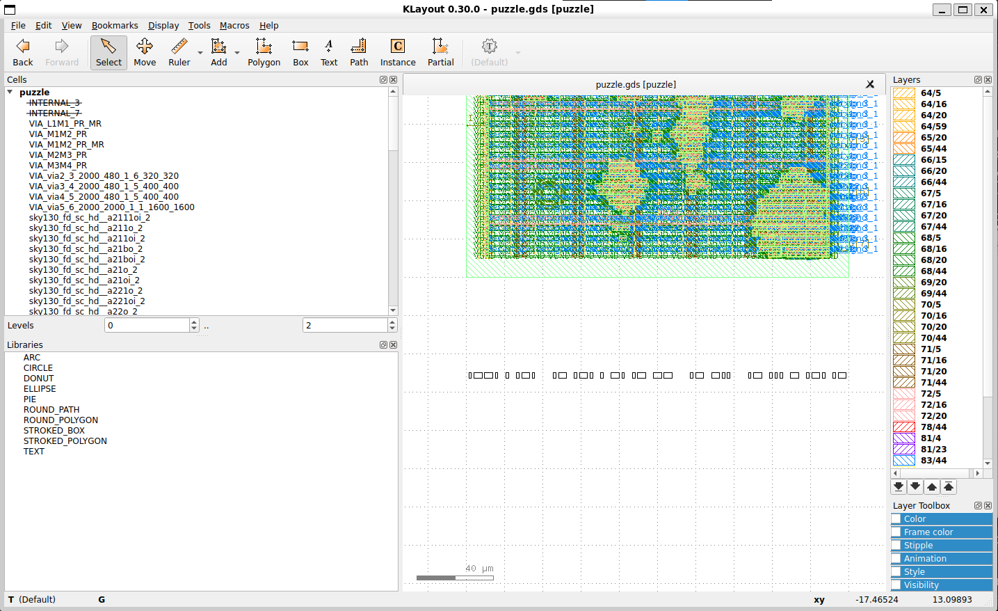
Looking back at the internal 3 and 7 cells in Klayout, the internal 3 is the small bar and the internal 7 is the long bar.

It looks a lot like morse code, and translating gives “PER ARENAM AD ASTRA”. It looks like Latin, from the “Per _ ad astra” phrase, and plugging it in to Google Translate spits out “Through the sand to the stars.”
Anyway, back to Magic.
It’s fairly easy to extract a netlist from the given layout. In fact, it’s basically a required step for performing layout vs schematic (LVS) which is especially important if you draw your layouts by hand as an analog layout designer or engineer.
Also, the lines have been marked with net labels for us, so it’s really just about figuring out what is going on in between.
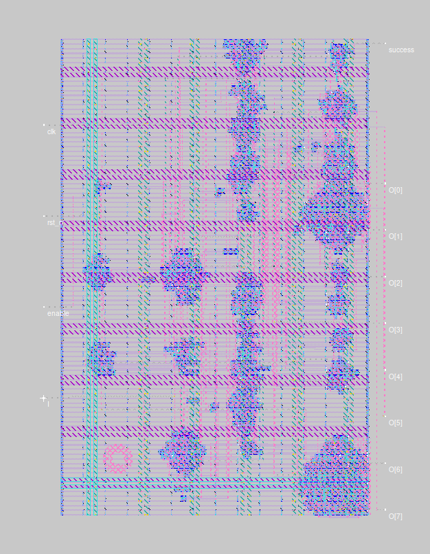
Looking at the top level design (with all the standard cells hidden), there seems to be no other layers in use besides the metal and via layers, which points towards what’s most likely a digital only design without metastable gates.
The Magic commands are very simple:
extract all
ext2spice lvs
ext2spice
Now, there should be a file called puzzle.spice in your working directory. Most of the content in the first half of the file is just describing the standard cells included in the PDK.
We can assume that the PDK implements the functions described. Looking at what’s extracted for each cell, we get pretty reasonable PMOS and NMOS arrangements.
What we’re really interested in is the top level subcircuit, which starts on the line that is
.subckt puzzle I O[0] O[1] O[2] O[3] O[4] O[5] O[6] O[7] clk enable rst_n success
This is where we get into the meat and potatoes of the analysis. That entire block is filled with statements like Xsky130_fd_sc_hd__inv_2_16 sky130_fd_sc_hd__inv_2_16/A sky130_fd_sc_hd__or4_2_5/B VPWR VGND VPWR VGND sky130_fd_sc_hd__inv_2 which, in order, means a inverter connecting another inverter to the second input of a 4 input or gate. This information is documented in the PDK. Using a short python script (that could be generated by a language model of your choice), the Xinstance node1 node2 ... model format can be turned into the Verilog model instance (.input1(.output1_wire) ...) format while simplifying away the cells that do no logic (such as decoupling and via cells). The PDK includes the cells as Verilog modules which is what I used for most of my simulations, but you could go down to Verilog gate primitives in this step if you wanted to.
I verified that it could run by writing a short SystemVerilog testbench that would trigger the inputs (I, clk, enable, rst_n) in the same pattern as the example inputs and verified that the output matched in a simulation I ran with iverilog.
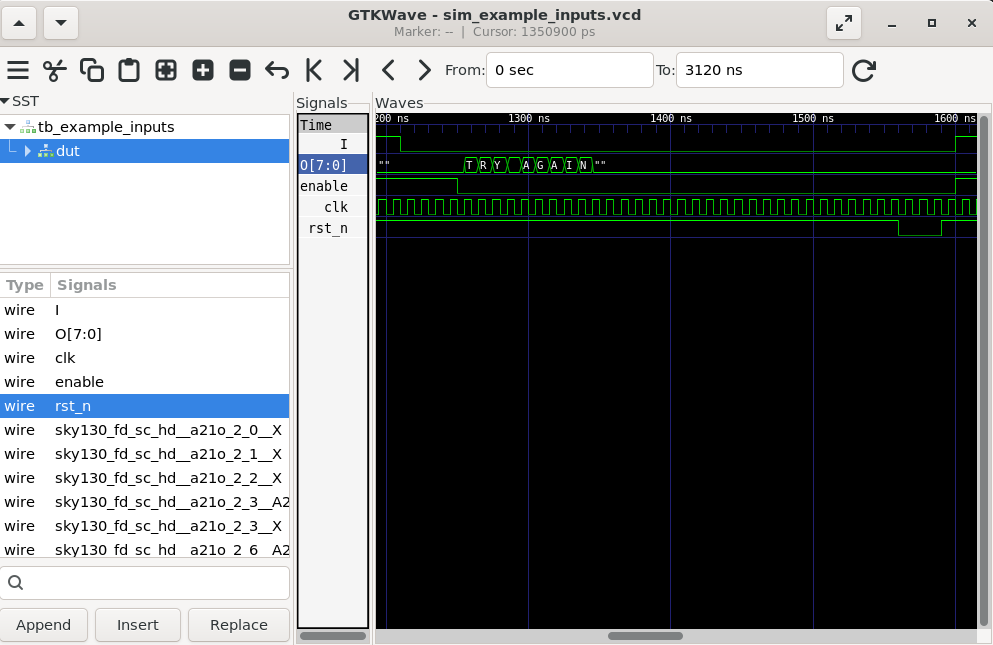
The key things to note is that the clock period is 10 ns, the reset is disabled in the third clock cycle, and the enable is one cycle after that. The output starts at clock cycle 125, even if you hold enable high afterwards.
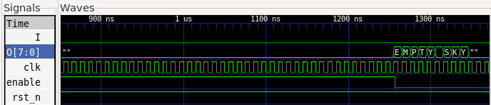
Trying with the input line held low, we get the string “EMPTY SKY”:
Trying with the input line held high, we get “BIG BANG”:
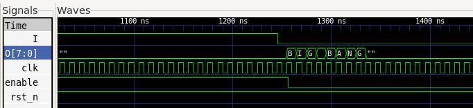
For both of these, the success line was held low.
So what we currently have are three pieces of text with a astronomy theme and no indication of a solution. It was at this point that I started looking further into the puzzle for more clues, and found this piece of text in the example_inputs.vcd

Looks like I have no choice but to try and wrangle the gates. Continuing the habit of using open source tools, I used Yosys, first to map the PDK logic cells into privatives by flattening, then using abc to turn it into easier gates to work with (and, or, inv) and opt, following with passes of opt_clean to remove unused cells. This decreases the number of gates we have at the cost of potentially making our reverse engineering a lot more difficult due to condensed gates. We get the following monstrosity:
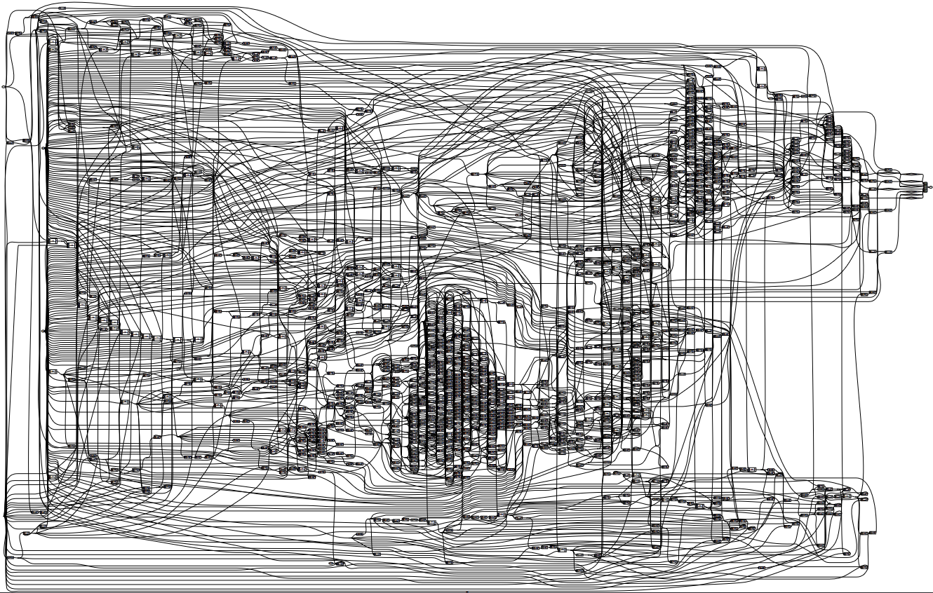
Assuming that enable is always high (since we only care about the logic flow while the chip is active) and hiding the clock signal and reset (to clean up the view), we get the following graph:
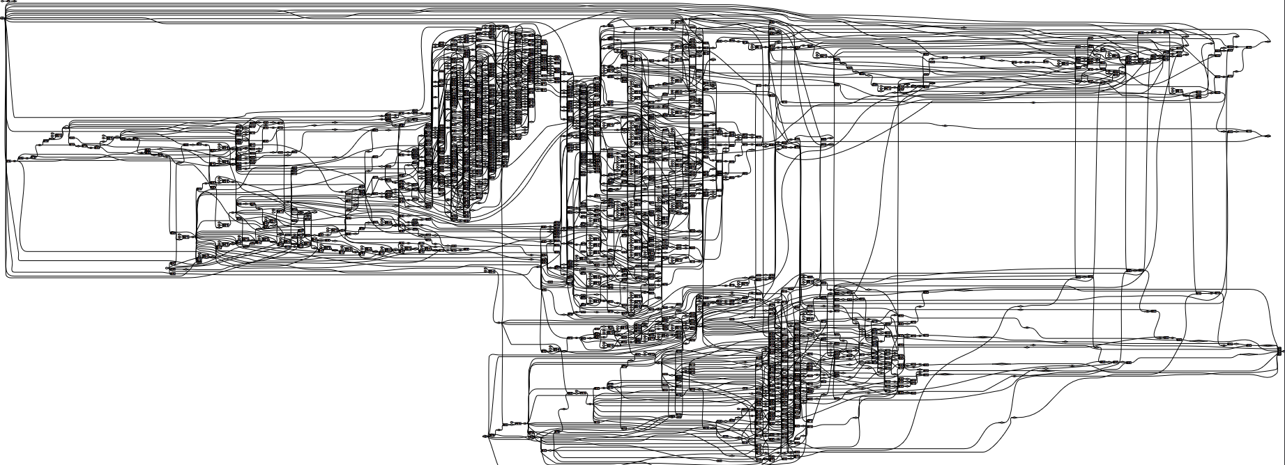
Still a nightmare. Using a bit of code to extract the nodes and edges in the dot file, I chose to dissect it in Gephi instead. Using a graph viz software such as this gives the benefit of being able to interactively play with different graphing layout algorithms in order to untangle the netlist like a big ball of virtual yarn.
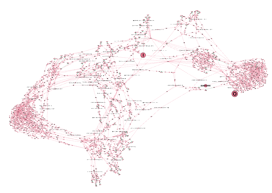
Shown above is one such untangling, with the input and output nodes increased in size, the non-storage nodes (any node that is not a flip flop) in pink and the storage nodes in green. Zooming into the nodes, we see a cluster of 4 flip flops separated from the rest of the circuit, which seems to indicate that this circuit has some secrets that could potentially be waiting for us.
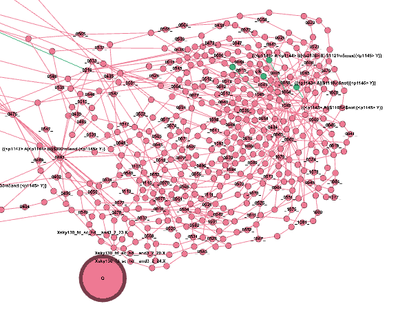
Cross referencing with the extracted Verilog, these are also unique in that they do not take the reset signal on input. This strongly suggests that these flip flops are part of the output generation sequence and not the checking logic. Which means that we could trick the output module by cutting away the rest of the flip flops and emulating the state. By doing this, we create a subgraph that has only 20 unique inputs, one of which is a clock.
This can be brute forced relatively quickly by a testbench, but the output result for some of these ends up being gibberish. The results that seem to be valid ASCII text are:
EMPTY SKY
TRY AGAIN
TWO NOT TOUCH
BIG BANG
We’ve seen most of these before, except for the third one. With a Google search of the phrase, there exists a puzzle game called Two Not Touch (also called Star Battle). The game is typically played on a 10x10 grid, with the following rules:
- There are two stars in each
- row
- column
- continuous region of squares surrounded shown by a dark border
- Stars cannot be next to each other in all directions
The input is only accepted for 121 clock cycles, but this is just enough to fit an 11x11 grid. Originally I had missed this as my test bench signals were slightly misaligned, but I ended up catching the issue in time.
With two and only two stars in each row, column, and group, there are 11 groups. However, there are 88 flip flops aside from the output generator. That’s not enough to store each cell value individually, so it’s more likely that these store fault conditions that our solution can’t make. One way to get at the logic is to work backwards by cutting the logic at the flip flops and working backwards from the success output. This creates a subgraph we can solve to figure out what the flip flops must be for success to turn high, which luckily enough is quite small.
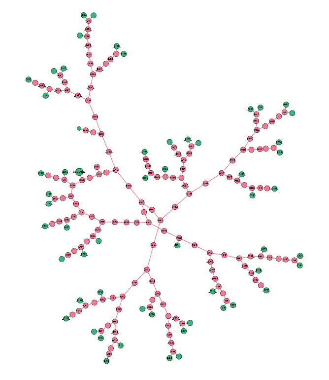
This looks quite scary when graphed with the full logic gate blocks, but it is actually fairly easy to work out by hand, since the bulk of the design is a ladder of and gates that feed forward.
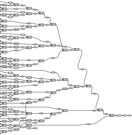
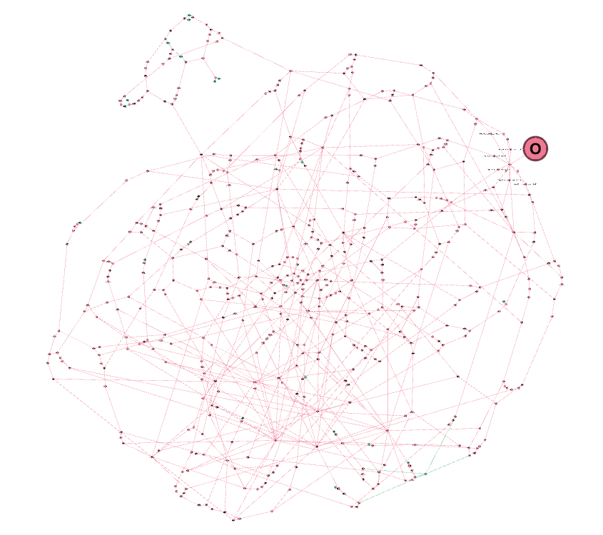
There are around 56 flip flops that need to be in a certain state to trigger success. Separating the input stage from the output stage, we get a porcupine netlist.
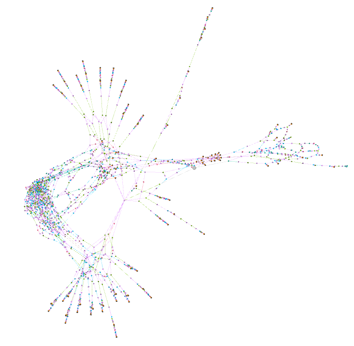
There are some structures here that are definitely identifiable as adders or a shift register. But there’s a huge mass of nodes that seem like a mess of logic. I spent some time looking at it but couldn’t reduce it to sensible logic, likely because of the aggressive optimization I did in Yosys. Now, it’s possible in SymbiYosys to solve nodes backwards as you would in formal verification, but that seemed more like work and less like a fun puzzle.
In my mind, a more interesting puzzle is brute forcing the combination. The search space for a 11x11 board is less than or equal to 31,197,434 according to this forum post, and I was getting a bit rusty in C. Using a C implementation and converted Verilog design, I got a successful match after a bit of waiting.
 . . . . . . . * . * .

 * . . . . * . . . . .

 . . . . . . . * . * .

 * . * . . . . . . . .

 . . . . * . * . . . .

 . . * . . . . . * . .

. . . . * . . . . . *

 . * . . . . * . . . .

 . . . * . . . . . . *

 . . . . . * . . * . .

 . * . * . . . . . . .
(* TWO STARS *)
Addendum
I had a chance to look at some of the approaches by other people, and pretty much all of them use a formal logic solver or manually trace through the gates. The closest yet I’ve found of someone that attempted a brute force solution said that it was impossible and moved on to using a formal solver, so I thought that I should detail why it isn’t as impossible as it seems (if you know that it’s a game of Two Not Touch).
The prior knowledge that you’ll need for this is that the input window is 121 clock cycles long, and that the input is a game of Two Not Touch. Granted, knowing that the input is a game of Two Not Touch is a feat in of itself, and would require examining the output generator or getting lucky with an input, like the following:
**.........
......*.*..
.......*.*.
..**.......
*...*......
.....*.*...
.....*..*..
.**........
.........**
....*.....*
...*..*....
If we treat the array as a bit array showing if a star is at that position or not, we can generate star arrays quite efficiently.
First, we start by generating rows. Each 11 bit row can only be 1 of 45 unique combinations, since each star has to be spaced out by at least a bit. This can be generated through the following code snippet:
uint16_t sequence;
uint16_t sequence_list[45];
int seq_i = 0;
for (int i = 0; i < 11; i++) {
	for (int j = i + 2; j < 11; j++) {
		sequence = (1 << i) | (1 << j);
		sequence_list[seq_i++] = sequence;
	}
}
Then, to assemble them into arrays, we need to know what other sequences are compatible with them (adding them won’t violate the adjacent or diagonal rules). Since we stored each row as a bit array, we can check if combinations are invalid efficiently through checking the bitwise AND and the bitwise AND with a left bit and right bit shift (ex. sequence_list[i] & (sequence_list[j] | sequence_list[j] << 1 | sequence_list[j] >> 1)).
After doing that, we can assemble each array by:
- Choosing one of the 45 sequences to start with
- Choosing one of the valid sequences that could continue off of it
- Checking if that sequence would place more than two stars on a column
- Choosing another valid sequence after that (step 2) until we get to 11 rows
This could be implemented in a short recursive function that returns early if there isn’t a valid row.
For efficiently counting the stars in each column, we can keep two 11 bit counters that specify if a column has more than one star and if a column has two stars. If adding a row would cause a column to have more than two stars (which we can check through a bitwise AND with the two star column count and the row), it’s invalid. After adding a row, the star column counts can be updated by bitwise ORing the row with the prior one star column count and bitwise ORing the prior two star column count with the row masked by the prior one star column count, ex:
new_cols_with_1 = (cols_with_1 | sequence_list[s]);
new_cols_with_2 = cols_with_2 | (cols_with_1 & sequence_list[s]);
There are a couple more optimizations you could do (such as checking if there are no columns that would need two stars by the 9th row or checking that no row sequence is used more than twice), but this should result in all 31,197,434 star arrangements generated in a couple of seconds.
Storing the valid arrangements by encoding them as their indexes in the unique row sequences, we get around a 250 MB file.
Now to test with the Verilog design. Unlike what I did, you could use a simulator with checkpointing (which is supported by commercial simulators like QuestaSim) and rewind at the row level when the board is incorrect, or even pass it through Verilator to increase simulation speed with a C/C++ implementation. I chose to do neither and just stuck with iverilog.
iverilog unfortunately doesn’t support checkpointing. So we’ll have to simulate each arrangement in full. There are some things that help, such as being able to feed in multiple arrangements after properly resetting the chip and having a success line that we can check, which reduce the setup and teardown compute time for each simulation. iverilog is also single threaded, so we can run multiple threads to check multiple arrangements in parallel. The way that we’ve stored all the arrangements is also fairly memory efficient and allows us to easily reconstruct it in the testbench itself.
Through batching the arrangement checks across 12 separate simulations running in parallel and letting them run overnight, I got the solution after around 8 hours of sim.
It’s not as efficient as using a solver, but it doesn’t use any tools that are more fancy than a C compiler, a Verilog simulator, and some computer time. And as a plus, it allows you to get your daily 8 hours of sleep (you didn’t forget that, right?).